February 27, 2020
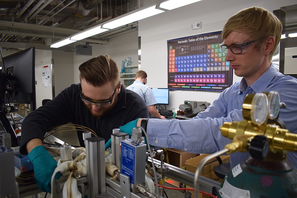
Chandler McCoy (left) and Asst. Prof. Matthias Young constructing the thin film coating reactor in Young’s lab at Mizzou.
As our electronic devices continue to grow in power and shrink in size, the semiconductor industry has been challenged to increase the number of transistors per unit. For 50 years, the industry has basically observed Moore’s Law, named after Intel co-founder Gordon Moore. He observed in 1965 that the number of transistors per silicon chip doubles every year. But researchers are beginning to say Moore’s Law is no longer a useful paradigm—a new architecture is needed for the computers and supercomputers of tomorrow. Mizzou Engineering Assistant Professor Matthias Young in the Department of Biomedical, Biological and Chemical Engineering is laying the groundwork for that new architecture.
Young, who received his bachelor’s degree in chemical engineering from Mizzou, worked as a postdoctoral researcher at Argonne National Laboratory prior to joining the faculty at MU in 2018. He now runs the Mizzou Thin Film Coatings and Materials Electrochemistry Lab, building on work he started at Argonne. His team’s current research projects focus on understanding and improving electrode materials for energy storage and water treatment applications.
“The type of chemistry my group uses to produce thin films is common in semiconductor device manufacturing,” he said. “The work in this recent paper points to a new frontier of flexible electronics. The chemistry we report is a new tool for people designing the next generation of semiconductor devices, a new tool for them to devise new architectures and new ways of designing and controlling matter on the nanoscale.”
In his new paper, “Molecular Layer Etching of Metalcone Films Using Lithium Organic Salts and Trimethylaluminum,” Young notes that advances in semiconductor device manufacturing are limited by our ability to precisely add and remove thin layers of material in multistep fabrication processes. Young was part of a team that has developed a new technique for the precise removal of metal–organic thin films deposited by molecular layer deposition (MLD), which they call “molecular layer etching.”
“This is an etching process that gives you layer by layer control of soft materials that would be required if you design flexible electronics from the ground up,” he said. Young said normal semiconductor devices are rigid—metal oxides and other hard, brittle materials built on a silicon wafer. He said manufacturers are starting to build flexible electronics, but the semiconductor chips are still rigid. For the chips to be flexible, one would need a flexible substrate and flexible dielectrics.
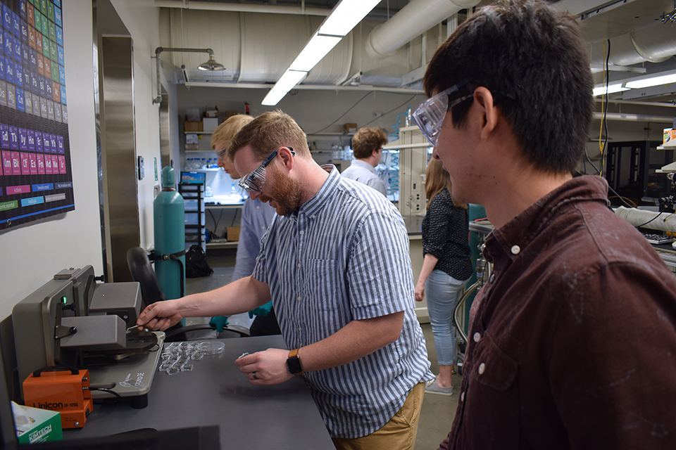
Matthias Young (left) and Xianglei Li (right) observe Quinton Wyatt performing a thickness measurement on a thin film coating using a spectroscopic ellipsometer.
“If you imagine this different paradigm of building flexible semiconductor devices from the ground up, you need to have analogous fabrication methods,” he said. “They’ve already developed fabrication processes for rigid devices, so we need those same sets of tools for flexible materials.”
Young says the lab he has built at Mizzou has similar capabilities to the lab where he did his research at Argonne, including a research reactor or a vessel where chemistry happens.
“You need very precise control over the chemistry, so we have unique instrumentation to control the reactions and study the chemistry as films are growing,” he said. “New technologies we can only dream of now may be achievable by building materials from the ground up atom by atom, and we have that capability in my lab here on campus at Mizzou.”
Young says his group is focused on thin film coatings for energy storage and water treatment, but those thin film coatings also could be used in semiconductor devices, coatings for drug delivery, changing the surface chemistry on medical implants, and many other applications.
“I’m open to collaborating with people in the UM System,” he said. “There are many applications for thin film coatings. We can deposit coatings on flat substrates, powders, and three-dimensional substrates with nanoscale control of the thickness and composition. I’m excited to connect with researchers to come up with new ideas.”
For more information about the new molecular layer etching process, read the news release from Argonne.